Designing Matter at the Nanoscale
How the Center for Integrated Nanotechnologies helps Los Alamos scientists transform theory into working materials.
- Kyle Dickman, Science Writer

“We didn’t have modulators,” Toni Taylor, a Los Alamos National Laboratory Fellow and physicist, says matter-of-factly, recalling work she began nearly two decades ago at the Center for Integrated Nanotechnologies (CINT) in Los Alamos. Modulators are the devices that allow scientists to control light—shaping its amplitude, phase, or frequency so it can carry information. Without modulators, terahertz light, a band of frequencies with enormous potential for communications and medical applications, could not reliably carry information. Without modulators, terahertz stubbornly remained one of the last regions of the electromagnetic spectrum to be technologically mastered.
Too slow for optics, too fast for electronics—the terahertz band lies between microwaves and infrared light, a narrow stretch of the electromagnetic spectrum wedged between two frequency regimes that have powered technological innovation for decades. In the 1940s, engineers developed radar by mastering microwaves with electronic circuits that could modulate the signals, and by the latter half of the twentieth century, physicists had built photonic devices to do the same with infrared and visible light for computation and communications. But unlike those light bands, when terahertz radiation hits the materials used to make conventional modulators, the waves mostly pass through: little absorption, little reflection, little control. That limitation became known as the terahertz gap, and it left significant technological potential untapped.
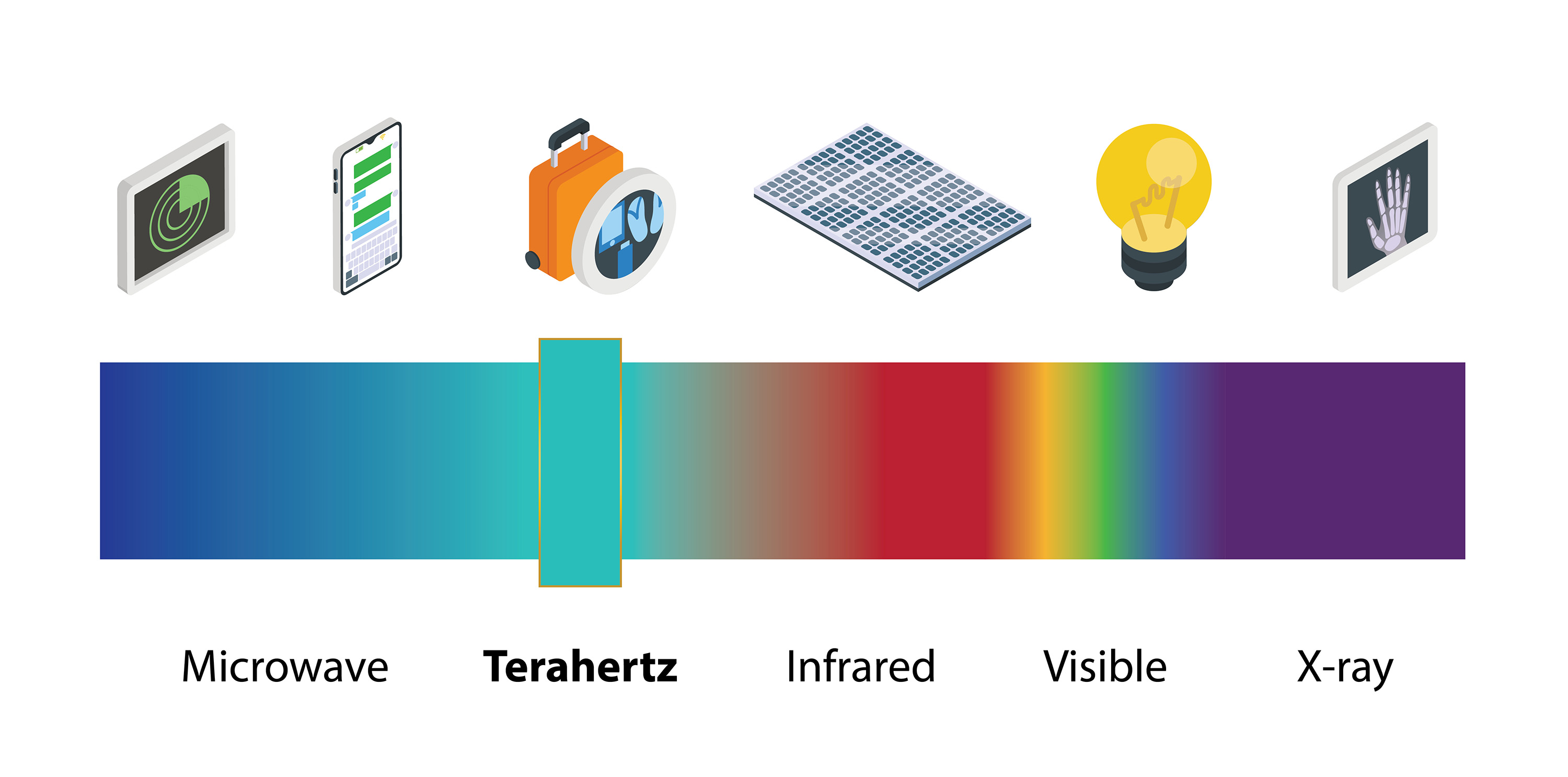
Terahertz waves oscillate trillions of times per second, hundreds of times faster than the microwave-frequency systems used in today’s wireless networks. In principle, that behavior means they could carry vastly more information than today’s fastest consumer networks. But communications is only part of the appeal. Like x-rays, terahertz radiation can penetrate many nonmetallic materials, but unlike x-rays, it doesn’t ionize atoms, meaning it doesn’t change the materials’ structure. In theory, that makes terahertz radiation well-suited to nondestructive probing of delicate materials, from biological tissue to concealed explosives. “There just weren’t good photonics devices there,” Taylor says. “At the time, neither naturally occurring materials nor manmade alloys interacted strongly enough in that band to control it.”
By the early 2000s, when Taylor and coworkers began working in the terahertz band, the computer revolution had pushed technology to an inflection point. Moore’s Law was still busy shrinking transistors, but devices had reached dimensions small enough that quantum effects shaped performance. Advances could no longer come from simply making components smaller. To keep accelerating computation, materials had to be designed down to the level of their very atoms.
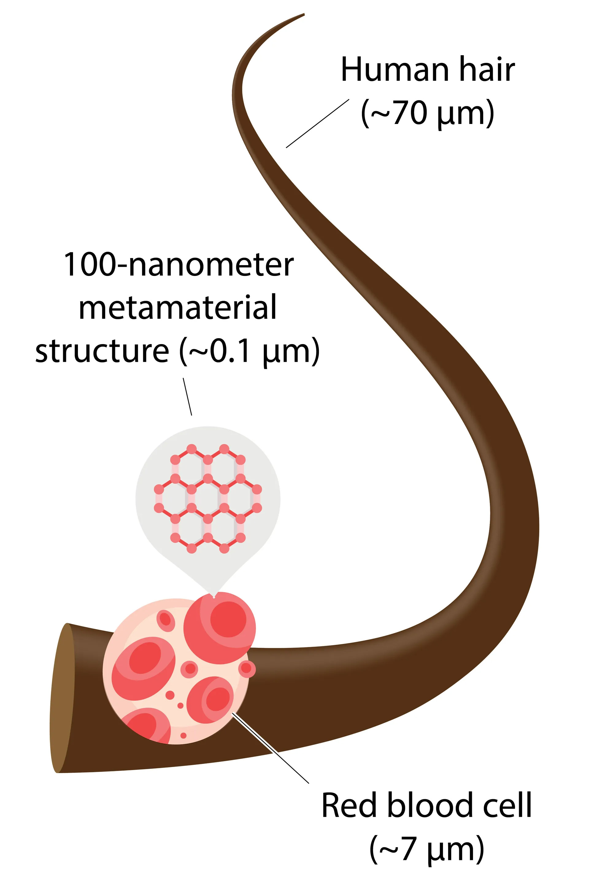
For the first time, nanoscale engineering, working at dimensions of billionths of a meter, where materials behave in fundamentally new ways, was becoming practical. Long before nano products were built, scientists could model them on supercomputers that predicted how electrons and electromagnetic waves would behave in such tiny structures. Cleanroom fabrication techniques refined by the microelectronics industry were building structures smaller than one hundred nanometers with remarkable precision, while scanning tunneling microscopes and atomic force microscopes made it possible not only to image the placements of individual atoms but, in some cases, to nudge them deliberately into place.
“For the first time, nanoscale engineering was becoming practical.”
All of these technological factors, plus the promise of the capabilities they enabled, led the Department of Energy’s Office of Science to create the Center for Integrated Nanotechnologies, a centerpiece facility among a national network of nanoscale research centers. Opened in 2004 and jointly operated by Los Alamos and Sandia national laboratories, CINT was built as a user facility, a place where scientists from around the world could propose ideas and gain access to specialized tools and expertise. Housed within this tightly integrated environment, researchers could move from theory to synthesis to fabrication to characterization—all at the nanoscale.
For researchers like Taylor, CINT turned the terahertz gap from an abstract limitation into an engineering problem. “All of the tools needed to develop the modulators were at CINT,” Taylor says. Her team’s work on the project began in earnest in 2006, when a postdoctoral researcher named Willie Padilla arrived at Los Alamos with expertise in metamaterials: artificially structured surfaces engineered to manipulate electromagnetic waves in ways natural materials cannot.
The way a material traditionally absorbs or reflects light is dictated by its atomic composition—the electronic transitions and vibrational modes built into its chemistry. Padilla’s insight was that they no longer had to rely on the electronic structure of naturally occurring materials to support a resonance at terahertz frequencies. They could engineer a material instead.
Using CINT’s modeling tools, he and his collaborators designed metallic patterns sized to resonate at terahertz frequencies: tiny, repeating loops and gaps etched into a thin film of gold. When a terahertz wave struck the patterned surface, its oscillating electric field drove the metal’s free electrons back and forth. If the geometry was right—if the loops and gaps were sized precisely for that frequency—the electrons would move in sync with the incoming wave. The energy in the terahertz waves that would otherwise have passed quietly through the material was briefly captured, scattered, or absorbed. Like radio antennas tuned to a single station, the gold resonators responded strongly only at the frequency dictated by their shape.
But this was still a passive response, like a filter or detector. The resonator device could isolate or suppress an individual frequency, but couldn’t change that frequency in real time. Without time-dependent control, it wasn’t yet useful for information transmission. To do that, Padilla, along with his coworkers Hou-Tong Chen, Richard Averitt, and Taylor had to find a way to modulate the signal itself.
The solution lay in setting the patterned metal resonator atop a semiconductor substrate. By injecting charge into that substrate—electrically or with an ultrafast optical pulse—the team temporarily increased its conductivity. That shift altered how freely the electrons in the resonators could oscillate. When the substrate became more conductive, the oscillations dissipated energy more quickly and the response weakened; when it was less conductive, the resonance sharpened. In practical terms, a static surface had become a controllable gate. A region of the spectrum long considered technologically awkward could now be modulated in real time. The work culminated in a 2006 paper demonstrating active control of terahertz radiation.
“We wanted to understand the materials and then design them to do the thing that we wanted them to do.”
What followed was not just a device, but a new way of thinking about matter: that it could be modified at the nanoscale to realize ideas once confined to theory. Taylor’s group went on to pursue higher-speed modulators, tunable filters, polarization rotators, and broadband converters. They extended the same nanoscale design principles to problems across national security and optical communications. More recently, collaborators demonstrated structures that can generate and steer terahertz radiation with unprecedented control. That approach has contributed to advances in security imaging seen at airports, materials diagnostics, and next-generation wireless research. Recent experimental terahertz systems achieved data rates exceeding 100 gigabits per second, far beyond typical consumer wireless speeds.
Terahertz modulation is only one expression of CINT’s broader vision. Across the Center, researchers have applied the same integration of modeling, fabrication, and measurement to problems ranging from quantum dots to structural materials. Victor Klimov and Jennifer Hollingsworth engineered quantum dots whose optical gain and emission can be tuned with atomic precision, advancing solar technologies, microelectronics, and quantum information science. Other Los Alamos teams designed nanoscale defect architectures to strengthen materials and built atom-scale emitters matched to fiber-optic telecommunications bands. Each effort differs in application, but they share a methodology enabled by CINT: design at the nanoscale, fabricate precisely, measure rigorously, iterate quickly.
“We wanted to understand the materials and then design them to do the thing that we wanted them to do,” Taylor says. The science has advanced since the early days of terahertz modulators. The ambition remains the same: to design matter itself.