
The 60R flight path provides a high-energy pulsed neutron beam generated by spallation of the 800 MeV LANSCE LINAC proton beam on the WNR tungsten target (Target 4).
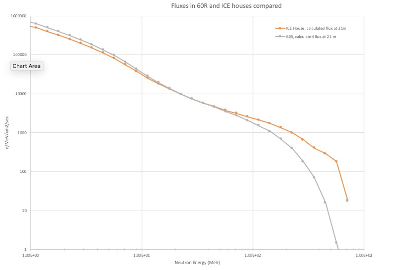
Neutrons emitted at approximately 60° relative to the proton beam travel along a flight path of about 19 m, enabling precise neutron energy determination using the time-of-flight (TOF) method. The short proton pulse width (≲1ns) provides excellent timing resolution, supporting energy-resolved measurements over a broad fast-neutron range from 1MeV to approximately 400MeV (see Fig. 1).
The 60R beamline offers approximately 4m of usable experimental space along the beam axis for detector systems, imaging setups, or irradiation studies. Collimation apertures allow the neutron beam spot size to be adjusted from about 6mm (0.24in) to 114mm (4.5in), providing flexibility to accommodate different experimental configurations.
The 60R flight path supports a broad range of experimental capabilities:
- Energy-resolved neutron imaging and radiography using time-of-flight techniques
- Radiation effects testing of microelectronic and semiconductor devices
- Neutron transmission measurements for nuclear cross-section studies
- Detector characterization, calibration, and performance validation
Fast Neutron Radiography at 60R
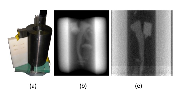
Neutron radiography is a non-destructive imaging technique based on neutron attenuation through matter. Unlike X-rays, neutron interaction cross sections depend primarily on nuclear structure rather than atomic number, providing enhanced sensitivity to light elements such as hydrogen, lithium, and boron, while maintaining strong penetration through dense structural materials, including steel, uranium, and tungsten. This complementary contrast relative to X-ray imaging enables visualization of internal structures (see Fig. 2), including fluid distributions, voids, cracks, and material interfaces in complex assemblies.
Neutron computed tomography (neutron CT) extends this technique by acquiring radiographic images at multiple angles and reconstructing a 3D volumetric image of the object. Neutron CT is particularly effective for visualizing hydrogen-containing materials embedded within metals and enables detailed internal characterization of multi-material systems.
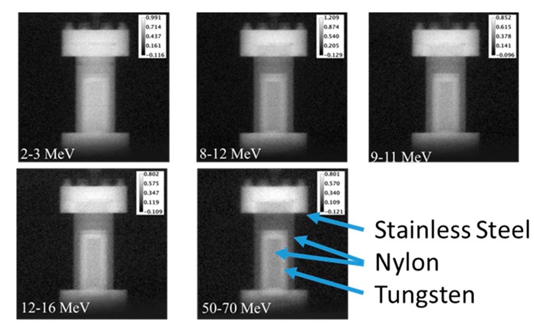
At WNR 60R, the pulsed neutron beam enables energy-resolved radiography via time-of-flight, allowing image contrast to be analyzed as a function of neutron energy.
Event-mode imaging detectors that combine scintillators with fast photodetectors or pixelated sensors provide nanosecond-level timing resolution, enabling simultaneous spatial and spectral imaging. These capabilities support applications in nuclear fuel characterization, materials science, and dynamic studies of radiation-induced changes in materials.
At WNR 60R, the pulsed neutron beam enables energy-resolved radiography via time-of-flight, allowing image contrast to be analyzed as a function of neutron energy. Event-mode imaging detectors that combine scintillators with fast photodetectors or pixelated sensors provide nanosecond-level timing resolution, enabling simultaneous spatial and spectral imaging. These capabilities support applications in nuclear fuel characterization, materials science, and dynamic studies of radiation-induced changes in materials.
Neutron Radiation Effects Capability
Due to high demand for beam time at the WNR ICE facilities (FP30L and FP30R) from industry users, availability for academic and non-proprietary experiments may be limited. The 60R flight path provides complementary capability and expanded access for radiation effects research on electronic components and systems.
Although the neutron spectrum differs from that in the terrestrial environment (see Fig. 1), the broad fast-neutron energy range may be well suited to investigating neutron-induced failure mechanisms and mitigation techniques that do not require the exact atmospheric neutron spectrum.
These measurements also support fundamental studies of neutron–matter interactions in semiconductor materials and contribute to improved understanding of device-level susceptibility in microelectronics.