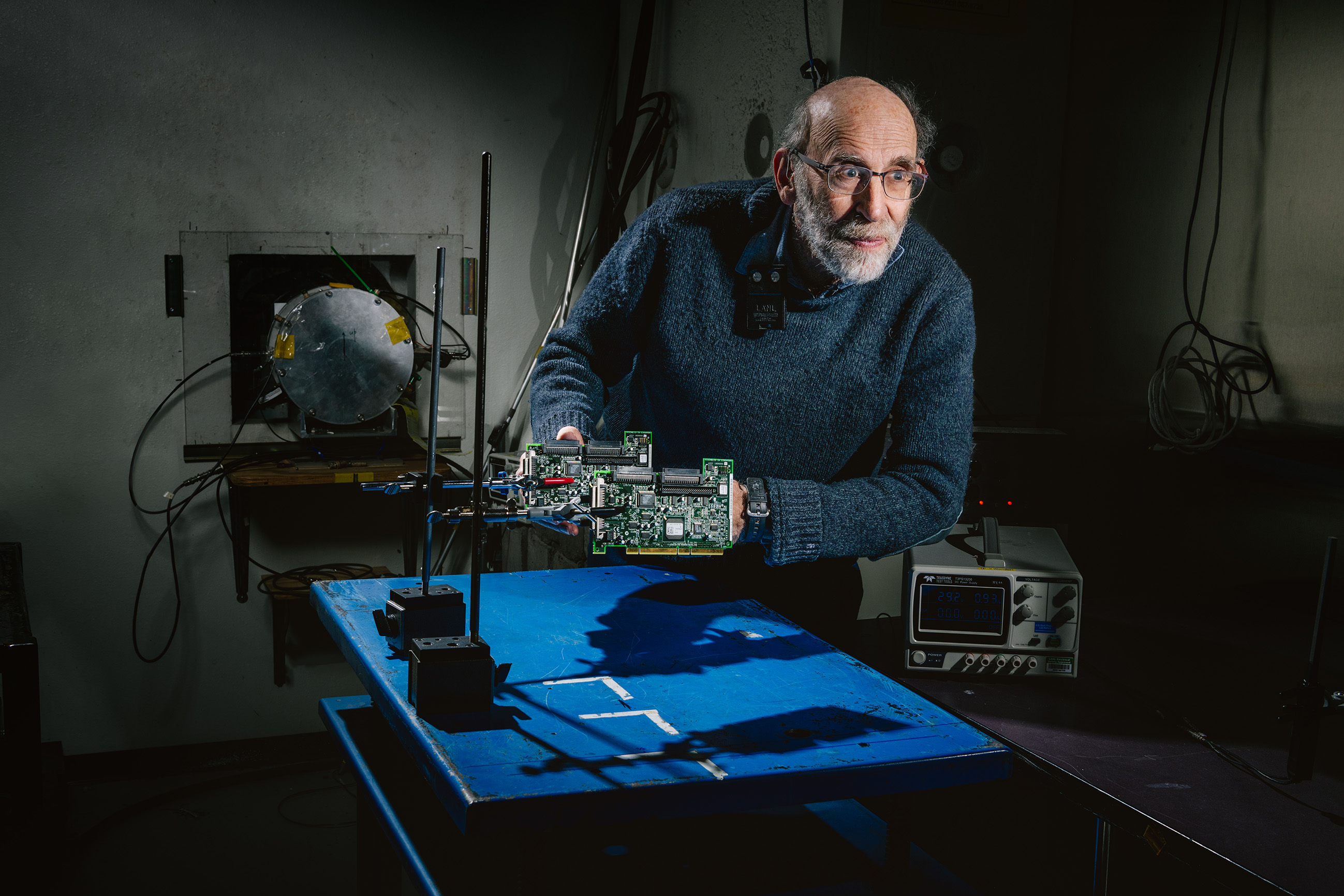
ICE-I reproduces the atmospheric neutron environment generated by cosmic rays to conduct accelerated neutron testing of semiconductor devices
The shape of the neutron spectra on the 30L flight path at Target 4 at the Weapons Neutron Research (WNR) facility at LANSCE is very similar to the neutron spectrum produced in the atmosphere by cosmic rays but with a neutron flux of over a million times higher.
Many industry, laboratory, and university researchers have used this facility to qualify and test semiconductor devices for single-event effects.
It is located on a flight path at 30° to the left of the Target 4 neutron production target. The neutron spectrum for this area is very similar to the terrestrial neutron spectrum produced by cosmic rays hitting the atmosphere and ranges from approximately 1MeV up to approximately 600MeV.
Because the ICE-I neutron spectrum is similar to the terrestrial neutron spectrum, one can predict the failure rate of a device in a particular environment (neutron flux) by just scaling the flux intensities. The integrated neutron flux for the ICE-I area above 1(10)MeV is 2.4 x 10⁶ (1.2 x 10⁶) neutrons/cm2/sec.
Details of the testing facility and testing procedures are in the Los Alamos High-Energy Neutron Testing handbook.
Effects of Neutrons Produced in Space
Neutrons are produced by galactic and solar cosmic rays reacting with the nuclei in the upper atmosphere. Although most of the primary charged-particle components of the cosmic-ray shower are absorbed by the atmosphere, neutrons are able to reach aircraft altitudes and below because they have no charge. These incoming neutrons penetrate semiconductor devices and collide with the atoms in the material, causing charged recoils (from neutron/atom collisions) and the production of secondary particles (protons, electrons) that deposit charge and energy in the devices. This charge deposition can initiate single-event effects in semiconductor devices that can seriously affect device performance.
Single-event effects include single-event upsets (SEUs), multiple-event upsets (MEUs), single-event latchup, single-event burnout, and gate rupture.
- SEUs occur when a memory location changes its state because of charge deposited by an energetic particle. Although this type of failure may be corrected by error checking, increased costs and a loss of performance are associated with this solution.
- MEUs, where several memory locations are altered, have been measured to be a few percent of the single-event rate. MEU failures may be more difficult to correct than SEUs.
- Failures such as latchup in which a device ceases to function are significantly less frequent but may be more serious because they usually require turning the device off and then on to eliminate the latchup.
In some cases, the devices may even have to be replaced. Other more serious failure modes occur in high-power devices in which a neutron can initiate a cascade of charged particles that causes these devices to draw large currents—possibly permanently damaging them as a result.
The failure rate in these devices strongly depends on the amount of applied voltage. The failure rate increases dramatically above a critical threshold voltage that may be significantly less than the rated voltage of the device.
Testing Semiconductor Devices at Greatly Accelerated Rate
An experimental area dedicated to accelerated neutron testing is located on the 30°L (left of the incident proton beam) flight path and also on the 30°R flight path at the high-energy neutron source at LANSCE.
The shape of the neutron energy spectrum on these flight paths is comparable to the naturally occurring high-altitude neutron spectrum (multiplied by 3 x 10⁵) in Figure 2.
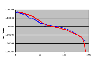
As shown in this plot, the shape of the LANSCE spectrum is very similar to the cosmic-ray-induced neutron spectrum but more than five orders of magnitude more intense. The integrated neutron flux above 1MeV is approximately 106 neutrons/cm2/s. This large neutron intensity allows testing of semiconductor devices at a greatly accelerated rate in which one hour of exposure at LANSCE is equivalent to more than 100 years of flight time.
The shape of the neutron spectrum may be altered by placing material such as polyethylene in the beam. This material serves as an absorber, allowing a greater percentage of higher-energy neutrons through to the test object as lower-energy neutrons are scattered by the hydrogen atoms in the material.
The shape of the neutron spectrum can be altered by adding various amounts of polyethylene absorbers in the neutron beam.
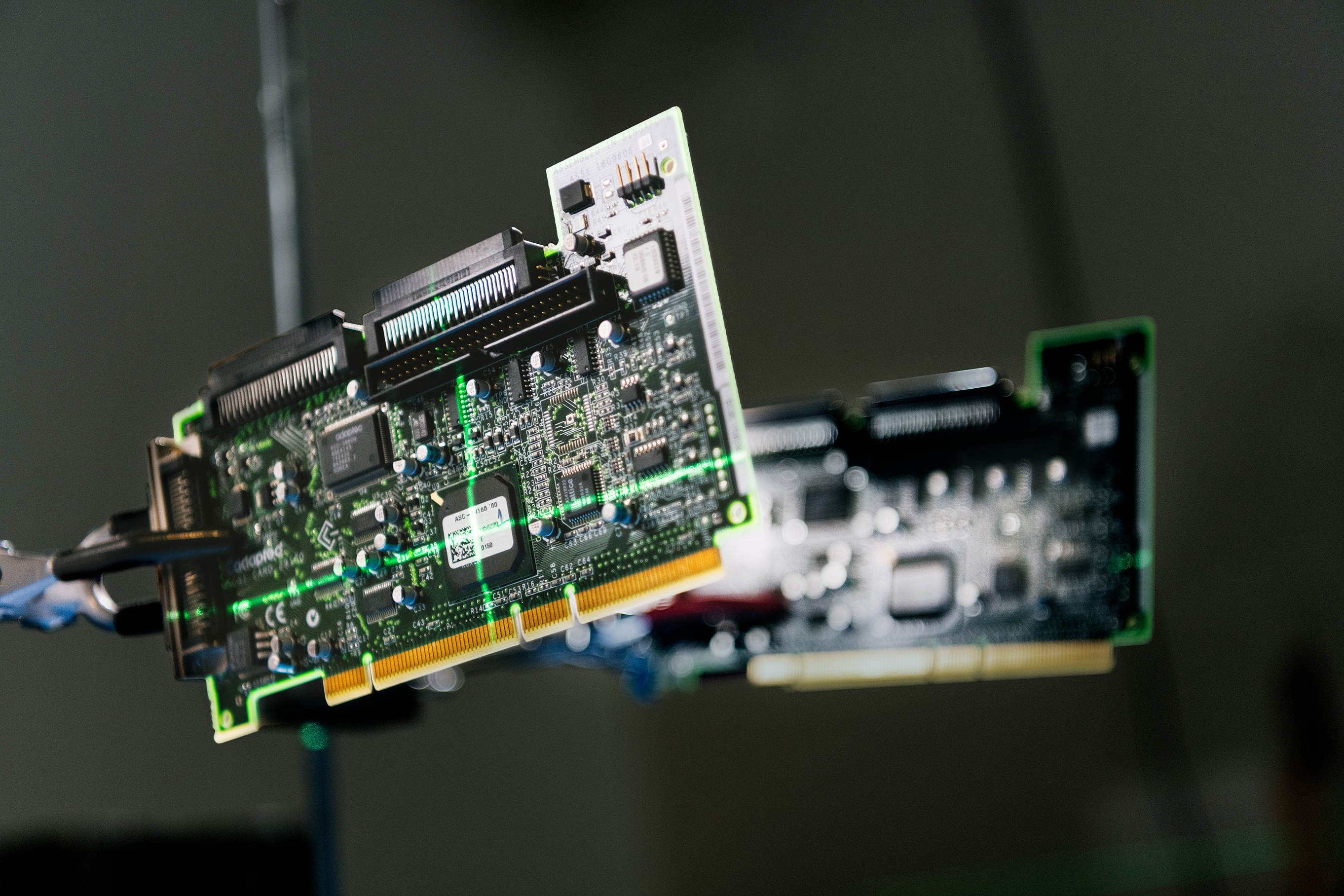
Semiconductor devices under test are placed in the neutron beam in open air. The neutron beam is collimated to a diameter of approximately 1-8cm at the test location. Because the neutrons are not strongly absorbed by the device and the supporting boards, several devices may be placed in the neutron beam at once, one behind the other.
The testing buildings have a shield wall that separates the irradiation and data areas and allows experimenters to move between the beam and the data-acquisition areas without going outside. An access road into the east side of the facility yard allows for easy transport and setup of equipment.