The ICE House Heats Up
New devices for aerospace engineering are irradiated at a special Los Alamos facility to see how well they withstand natural cosmic radiation.
- Eleanor Hutterer, Editor
Download a print-friendly version of this article.
Look into the cockpit the next time you board a plane, and you won’t see old-fashioned dials and gauges—you’ll see computer monitors and digital displays. Since the 1970s, commercial and military aircraft have steadily transitioned their controls and instrumentation from analog to digital, adopting a ‘fly-by-wire’ configuration that relies on electronics to control the plane and report vital flight data.
From airplanes to photo frames, just about everything these days has a digital component. Compared to their analog forebears, digital displays are easier to read, can show more information across a smaller space, and tend to require less maintenance. However, because they rely on semiconductor transistors—tiny switches that control the logic and memory of microchips via careful flow of electric charge—anything digital is vulnerable to the charge-disrupting effects of natural radiation. A key part of the product development pipeline for microelectronics is radiation hardness, or rad-hard, testing. This determines what damage is caused by radiation so the product can be hardened, or engineered, to resist such damage. This is particularly important for aerospace and avionics: as altitude increases, radiation increases. The higher you fly, the hotter the sky.
Los Alamos helps microelectronics-makers ensure their products are as rad-hard as possible by irradiating the heck out of prototypes in controlled and specific ways. The Irradiation of Chips and Electronics facility, called the ICE House, is an experimental area at the Los Alamos Neutron Science Center (LANSCE). It’s the only place in the country where this crucial work is done. By helping to ensure the flight-readiness of new aerospace and avionics components, the ICE House improves public safety and drives basic science while also supporting national security.
A rain of cosmic radiation
“Just one neutron can stop a train,” says Steve Wender, Los Alamos physicist and head scientist for the LANSCE Radiation Effects user program at the ICE House. “Theoretically, anyhow; in practice, these things are built with backups and safeguards in place. The point, and the reason for those safeguards, is that cosmic rays plus atmosphere equals neutrons, and just one neutron can cause a fault in a semiconductor device.”
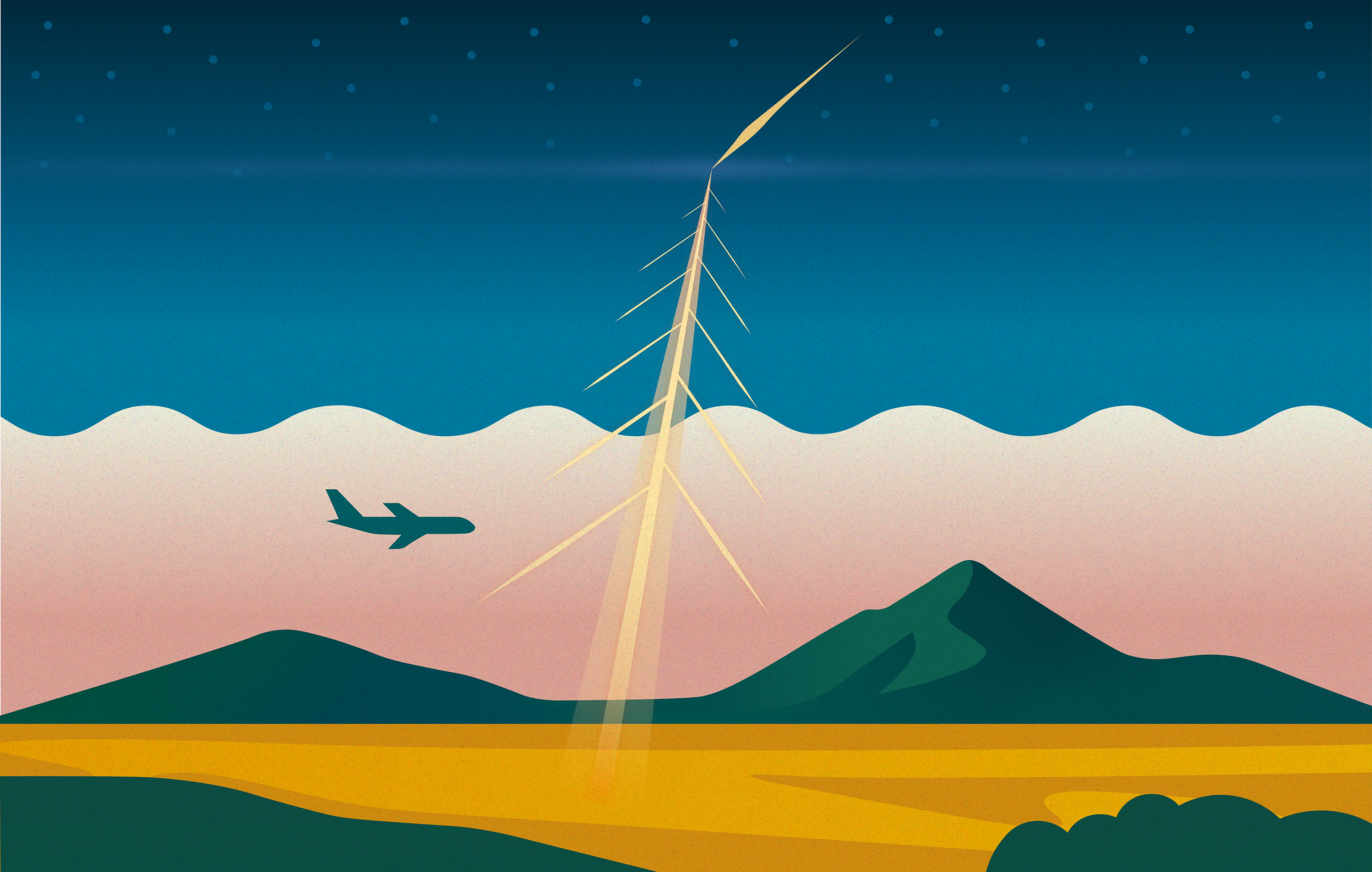
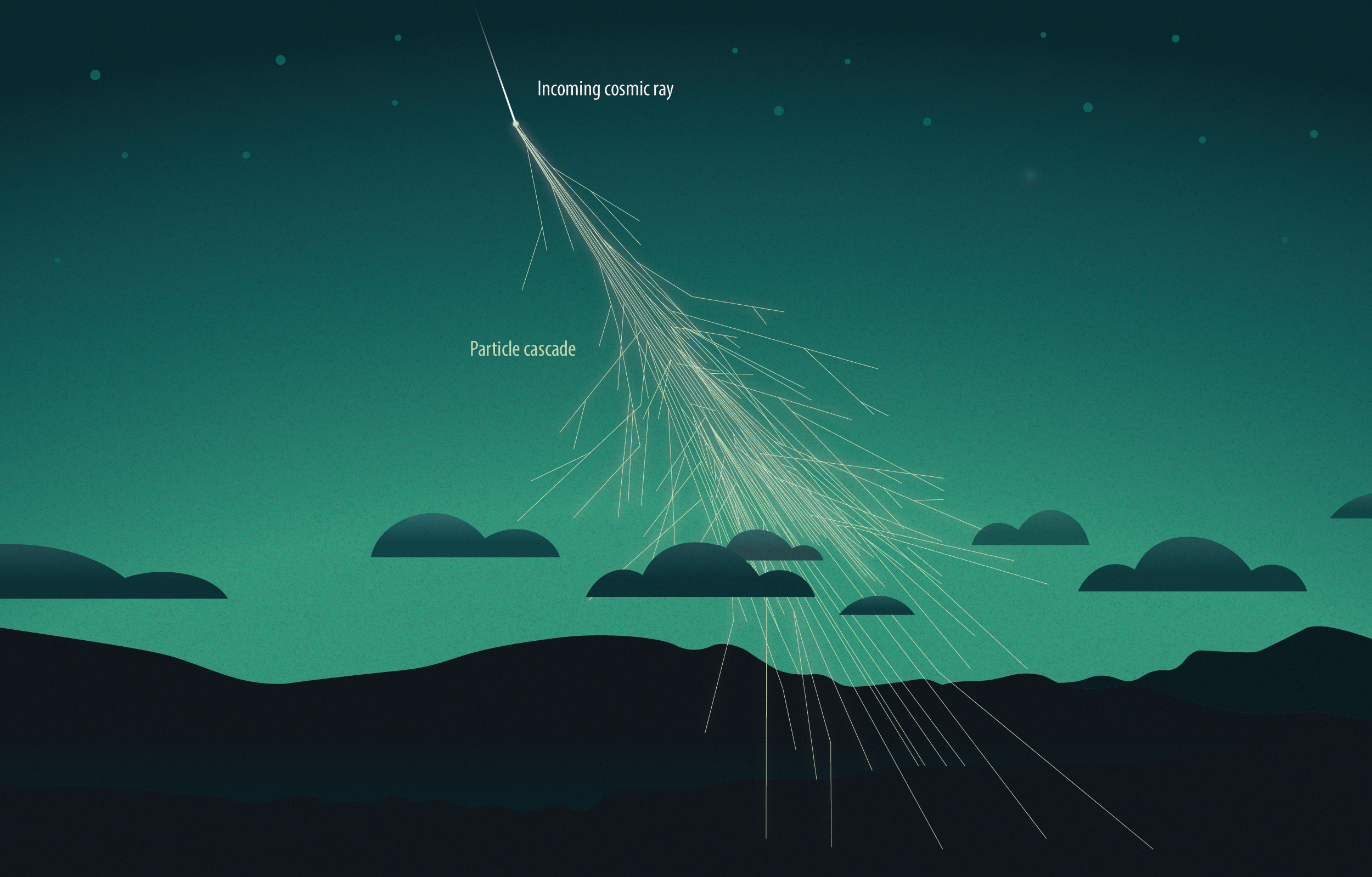
Cosmic rays are particles—mainly protons—that enter Earth’s atmosphere from space. (Cosmic rays can also be other subatomic particles as well as helium nuclei and occasional heavier nuclei). These particles travel from various sources in space—some nearby, like the Sun, and some very far away, like exploding stars in other galaxies—and rain down on Earth by the trillions every day. When a high-energy cosmic ray smashes into an air molecule in Earth’s upper atmosphere, both the cosmic ray and the molecule burst apart, sending all sorts of lower-energy particles off in all directions. These particles then crash into other molecules and burst those apart, spewing out even more, still-lower-energy particles. This cascade of collisions and particles is called an air shower, and it continues until all the energy of the initiating particle has dissipated. And it can be a lot of energy: the highest-energy cosmic ray ever recorded, dubbed the OMG particle, was a single proton that slammed into Utah in 1991 with all the power of a 62-mile-per-hour baseball.
Out of this jumbled air shower of protons, neutrons, electrons, positrons, pions, muons, neutrinos, and gamma rays, it’s neutrons that are most relevant to microelectronics in the atmosphere. And due to the cascading structure of air showers, there are a lot of neutrons flying around at the very altitudes where a lot of microelectronics also fly around.
Just one neutron can stop a train.
Air showers begin at the top of Earth’s atmosphere, between 80,000 and 115,000 feet up. All incoming cosmic rays will collide with an air molecule by 80,000 feet, meaning it’s just secondary particles from that point down. As the cascade continues towards Earth’s surface, more and more subatomic particles are released, reaching maximum particle density at about 65,000 feet. Commercial aircraft typically cruise between 30,000 and 40,000 feet because the air there is thinner and calmer, making for a smooth and fuel-efficient flight. But at that altitude there are 300 times more neutrons than at sea level, meaning a microelectronic fault that occurs once a year at sea level will occur nearly once a day at 35,000 feet.
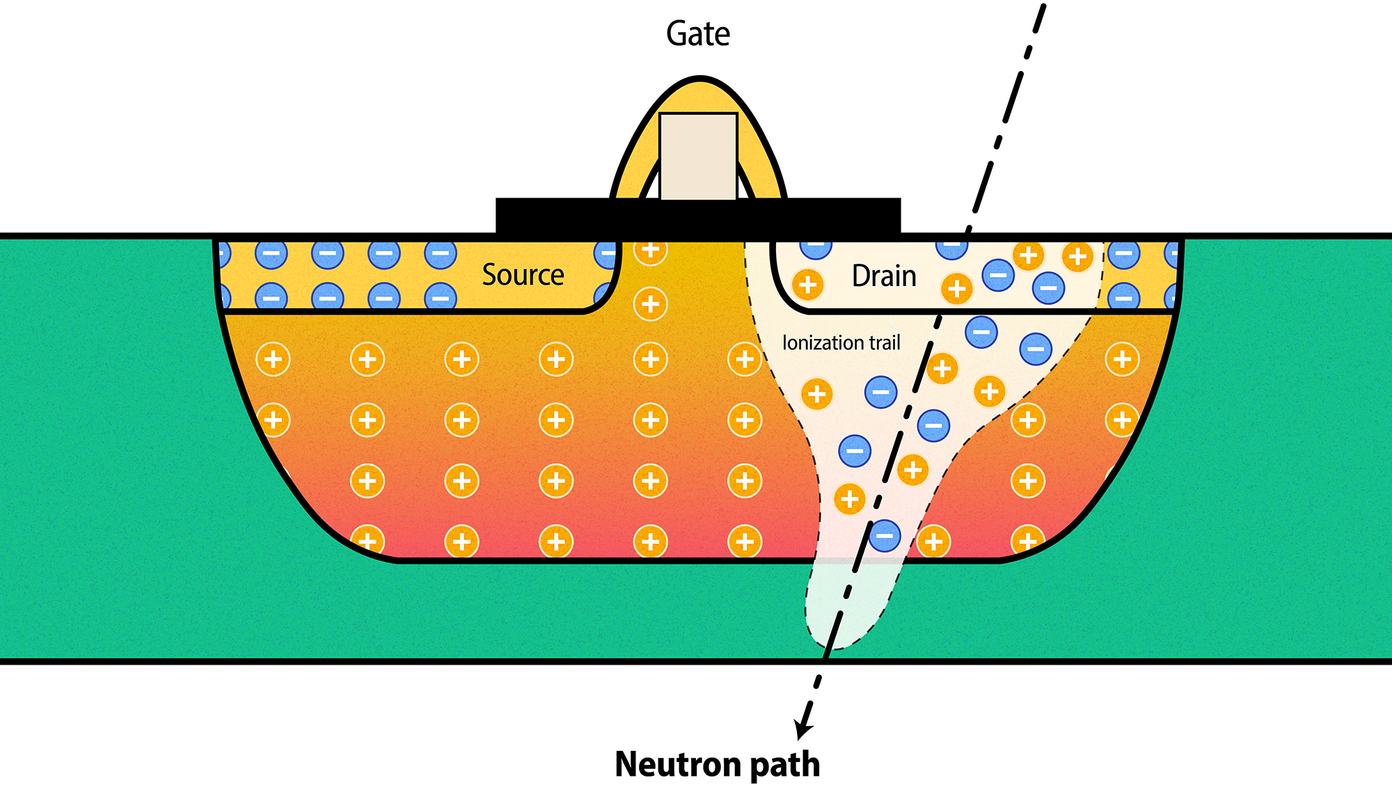
Because neutrons are uncharged (neutral), they travel unaffected through the atmosphere and magnetic fields. But if a neutron happens to collide with an atom in a semiconductor transistor, just like in an air shower, the collision can cause the release of secondary particles—some of which do carry charge. Transistors rely on a careful arrangement of nuclei within a semiconductor material to conduct electric current, and if a free-wheeling neutron whizzes through that careful arrangement, it can produce a chaotic streak of ionization in its wake, which deposits charge in the device. This charge interferes with the operation of the semiconductor device and can cause it to glitch or seize up.
Single-event upsets and the blue screen of death
A transistor is a device that can amplify electric signals by controlling the voltage passed through an electronic circuit, and transistors made from silicon are the fundamental building blocks of modern electronics. Silicon is an ideal material for a transistor because, in addition to being naturally abundant and thermally stable, it’s a semiconductor material that can easily be doped (modified) with charge-carrying atoms to control its ability to conduct electricity.
There are a lot of neutrons flying around at the very altitudes where a lot of microelectronics also fly around.
The three main parts of a semiconductor are the source, the drain, and the gate. The source and drain are made of n-type silicon, so named because it is doped with negatively charged atoms. Separating the source and drain is a body of positively charged, p-type, silicon. (Alternatively, a p-type source and drain can be separated by an n-type body). The gate sits on top and controls the electrical current. When the gate is open, an electrical current is applied and electrons flow from the source, through the body, and into the drain. When the gate is closed, electrons don’t flow, and the transistor is off. If a neutron collides with the transistor, electrons from the n-type zone can get ripped off and dropped into the p-type zone, disrupting the distribution of charge.
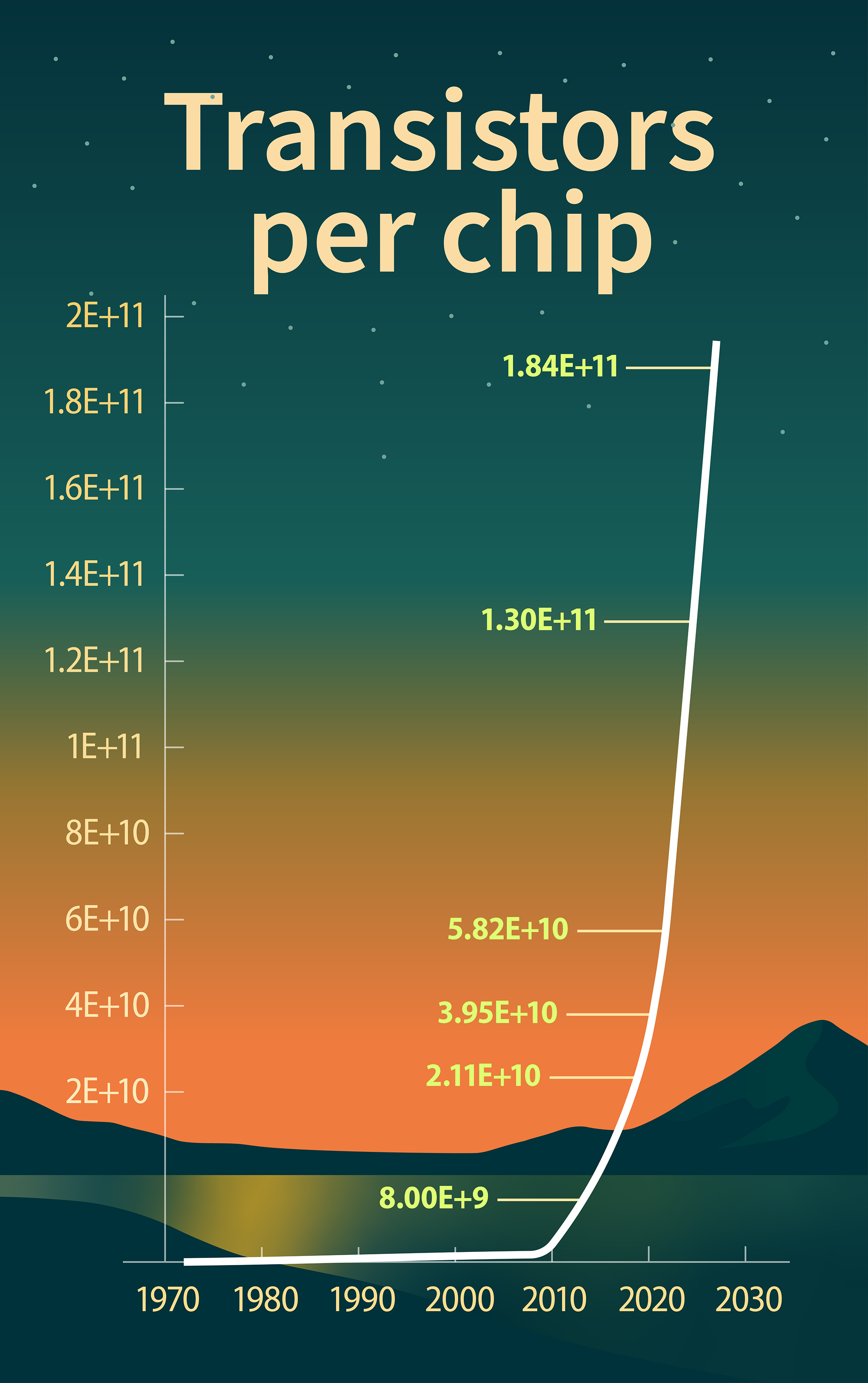
As transistors get smaller and smaller, they can become more susceptible to neutrons. In March 2025, the highest transistor count on a single consumer microprocessor chip was 184 billion. Special-use chips can have even more, into the trillions. That’s billions or trillions of chances for neutron-induced faults, called single-event upsets (SEUs), that can affect the memory or logic of the chip.
The most common type of SEU is a bit flip, where the fault occurs in binary digit memory element, or bit, and changes its state from 0 to 1, or from 1 to 0, corrupting the memory that the bit controls. Single bit flips can be fixed with error-correcting logic built into the code. A latch up is another possible SEU that is more serious than a bit flip. In a latch up, the transistor gets stuck in the closed position, causing a current surge that overheats the device. Sometimes powering off the device can fix it, but sometimes the damage is permanent. And then there’s the dreaded blue screen of death. Not necessarily a fatal error, as the epithet implies, the blue screen is a stop error displayed by some computer operating systems to warn the user of a critical issue. Although it’s rare for a neutron SEU to be fatal to a system, it can happen. One neutron can cause SEUs in multiple transistors, affecting everything downstream of those transistors.
Most often, damage accumulates over time, and it takes many SEUs before the effects are apparent. Ever notice your aging device getting hotter faster or its battery draining more quickly? These can both be the result of accumulated damage in the device’s transistors. The amount of radiation damage it takes to get to that point, the energies of the neutrons causing the damage, and the types and frequencies of errors that occur—this is the sort of information that the ICE House delivers.
Getting hot
“One hour of irradiation in our beam is equivalent to a hundred years of natural exposure at aircraft altitude,” explains Wender. “Most major companies have tested parts here to predict their performance in natural environments and to find the limits of reliability. Here, they can learn in a few hours what would otherwise take them years.”
One hour of irradiation in our beam is equivalent to a hundred years of natural exposure at aircraft altitude.
In the early 1990s as fly-by-wire was taking hold, so too was concern within the avionics industry about how natural radiation could affect electronics. At the same time, neutron research at Los Alamos was growing, as evidenced by the 1995 name change of the Los Alamos Meson Physics Facility to the Los Alamos Neutron Science Center. With the world’s most powerful high-energy neutron source in residence, LANSCE scientists were keen to develop new and valuable ways to use this unique resource.
The LANSCE experimental area with the highest-energy neutrons is the Weapons Neutron Research center. Here, high-energy protons from the LANSCE linear accelerator bombard a tungsten target, which responds by spewing out neutrons with energies ranging from about 0.1 MeV (mega-electronvolts) to more than 600 MeV. This energy range is virtually identical to the energy range of air-shower neutrons, so it was serendipitous when one of Wender’s colleagues, a neutron scientist turned aircraft engineer, recognized the potential and gave him a call.
“The first experiments in 1992 were a little crude,” admits Wender. “We set them up outside, in the open air, but it worked quite well. Once we knew it worked, we built some small shacks. Then, in 2004, we built an actual building.” And the need has continued to grow. By 2012, the ICE House flight path was so oversubscribed with customers across the spectrum of electronics and avionics manufacturers that the Lab developed a second flight path, called ICE II. The energy spectrum for ICE II neutrons is the same as at the original ICE House, but the flux, or concentration of neutrons hitting a particular spot at any given time, is about two times higher at ICE II. No other neutron facility can offer this intensity with a spectrum that so closely matches the natural spectrum. Indeed, there are so many neutrons with such low absorbance that many chips can be lined up, one behind the other, and irradiated all at once.
The digital device can be off or on during irradiation, depending on the question being asked. If, for example, you are interested in bit flips, you can write a bit pattern to memory, zap it, then turn it on and see if the memory holds. If so, great; if not, the bit has flipped. Or, if you are interested in distinguishing the effects of neutrons at different energies, for certain devices, you can use time-of-flight methods to determine the energies of the worst offenders. Here’s how that works: Neutrons are emitted from the source in pulses, which sort of spread out during their flight from the source to the sample, with the highest energy neutrons leading the group and the lowest energy neutrons bringing up the rear. When the chip glitches, the time of upset is tagged to within a few billionths of a second. This timestamp tells the time it took the neutron to travel from the source to the chip, which corresponds to the neutron’s energy. A typical static random access memory chip will experience about 1200 SEUs per hour while being irradiated. The customer then takes this data, adds information about the neutron flux in the environment of interest, and can accurately predict the performance of their device. Then they must decide what steps to take to improve it.
Rad-hard by design
There are different ways that transistors and microelectronics are engineered to resist damage from natural radiation. Materials-level maneuvers include using materials that are less susceptible to ionizing radiation, incorporating shielding materials around sensitive components, and employing creative layouts to resist damage. Configuration-level maneuvers include building error-detection and correction into the code, circuit redundancy within components, and component redundancy within systems. Virtually all modern commercial and military fly-by-wire control systems are triply or even quadruply redundant in their electronics. Whatever strategies the microelectronics companies devise, new parts must come to LANSCE for rad-hard testing.
The ICE flight paths are the busiest at LANSCE. Between the two existing flight paths there are 306 days of beam typically available per year, and even when running 24 hours a day, it’s still not enough to meet demand. So, negotiations are presently underway to build a third ICE flight path at LANSCE.
No other neutron facility can offer this intensity with a spectrum that so closely matches the natural spectrum.
“In addition to commercial avionics, there are commercial terrestrial applications—think cell phones, big-data centers, self-driving cars, supercomputers—as well as programmatic applications—think fighter aircraft, drones, cruise missiles—and the Department of Defense recognizes the need for more testing capacity,” explains Wender. “It’s not really a new flight path, it will be a modification to an existing path, dedicating it to component testing.”
Another up-and-coming project is a proton facility for testing radiation effects in the space environment. At aircraft altitude and on the ground, the main concern is neutrons, because Earth’s atmosphere provides pretty good shielding against protons—roughly the same as 10 feet of concrete overhead at all times. But in space, there are more high-energy protons, which can knock a silicon atom out of place, causing electrical current to either get trapped in a transistor or else leak out. Every once in a while, the Sun blows its top and emits bursts of cosmic rays that temporarily increase background radiation levels by a factor of 1000. We see them from Earth as solar flares and Northern lights. Though not predictable, these bursts do send out warnings: it takes 8 minutes for the associated light to reach Earth, and slightly longer for the particles themselves. It’s enough time to temporarily shut down any satellites in harm’s way. Wender is collaborating with scientists at Honeywell and NASA to build a proton detector that will fly in high-altitude airplanes to measure and observe these extreme space weather events, with the goal of improving rad-hard design for microelectronics.
In 1992, when Wender first started irradiating chips at the ICE House, the microchip market was heating up, and it’s only gotten hotter. The number of electronic devices in the world has increased exponentially and so too has the number of transistors per chip. As big data gets bigger and microelectronics get smaller, humanity must rely more than ever on our digital devices. Thanks to Wender and his ICE House colleagues working to keep digital devices reliable, we can.
People Also Ask:
- What is a single event upset? A single event upset, or SEU, is a transient error in a digital device, caused by natural radiation, that affects the memory or logic function of a microprocessor. Many SEUs are non-destructive and can be reversed by resetting the device, but some can cause permanent damage.
- What are cosmic rays used for? Cosmic rays are high-energy particles from space. They are studied to understand particle physics as well as the nature and history of the universe. They are also studied for the effects of their secondary particles, like muons, which are used in tomography, and carbon-14 atoms, which are used for radiocarbon dating.