Grappling with Graphene
The strongest and most conductive material known, in a layer just one atom thick
- Craig Tyler, Editor

Flexible thin-film touch-panel displays. Spray-on solar cells and extremely long-lasting batteries. Nanoelectronic computer chips and optoelectronic communications devices. Ion and gas transport membranes. Precision sensors and biosensors. All this and more, graphene can do.
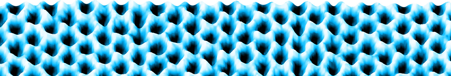
Graphene is made from carbon atoms arranged in flat, interconnected hexagonal rings, like chicken wire. Its simple, two-dimensional atomic structure gives it an unusual blend of electrical, mechanical, and optical properties. It is flexible and transparent. It conducts heat and electricity. It has special magnetic properties. And despite being lightweight, it is vastly stronger than steel. But its unique atomic structure is both a blessing and a curse. Because to unleash its tremendous potential, it must first be cheaply and reliably manufactured to be one atom thick and free of defects at the atomic scale. That is to say, the desirable material properties depend upon micro-structural perfection.
Graphene dimensions: one atom thick, roughly a million times thinner than a human hair. Distance between carbon atoms in hexagon structure is 0.14 nanometers.
The trouble is, there’s no practical way to position all the carbon atoms perfectly. Graphene must be made with some sequence of macroscopic batch processes—heating and pouring and coating and dissolving and the like. The tiniest irregularity at any stage introduces performance-limiting defects into the final product. And even if researchers somehow manage to construct the graphene just so, they still must transfer it to its target substrate—whatever surface it’s supposed to reside upon, such as a thin-film display screen. Somehow, they must pick up, transport, and set down an invisible, one-atom-thick carbon sheet without altering it in any way.
Enkeleda Dervishi and her team at the Los Alamos Center for Integrated Nanotechnologies have developed a process to do just that. The process starts with a sheet of copper foil, heated to 1000°C in an inert atmosphere, into which she injects methane gas, or CH4. The high temperature dissociates the methane into carbon and hydrogen atoms, and the carbon atoms settle onto the copper foil, naturally forming hexagonal rings. At this point, however, it’s not just graphene; it’s graphene attached to copper foil. Getting the graphene off the copper and onto a target substrate, which will be used for various applications, is the tricky part.
The copper can be dissolved away with an acid wash. However, to transfer the graphene onto the target substrate, a different material is required—one invulnerable to the acid but vulnerable to something else the target substrate can withstand. Two commonly used transfer materials are thermal release tape, which is sticky tape that peels away with heat, and PMMA, or “poly(methyl methacrylate),” which is a plastic that can be dissolved in acetone. Unfortunately, both materials leave a residue on the graphene surface and are too expensive and time consuming to be used at production scale (even if the residue were deemed tolerable for a particular application).
Dervishi needed a better transfer medium and decided to try a plastic resin commonly known by its former trade name, Formvar. She chose Formvar because it can be produced and applied smoothly as a liquid and can be dissolved completely and easily in chloroform, without affecting the graphene. It is also durable enough to transport the graphene onto its target substrate, and it scales inexpensively for commercial use. In addition, it possesses sufficient flexibility to transfer the graphene onto its target substrate, properly adapting to any atomic-scale irregularities on the substrate’s surface.
Next, Dervishi and her students, Eric Auchter and Justin Marquez, set out to develop a reliable transfer procedure. They found that they could affix the Formvar to the graphene by simply dipping the copper-graphene sheet graphene-side down in a liquid Formvar mixture and allowing it to air dry. Then, handling the Formvar side only, they could lower the copper-graphene-Formvar stack into an acid bath to dissolve away the copper.
The total value of the global graphene materials market is tens of millions of dollars as of 2017.
After several washes in ultrapure water, the graphene- Formvar sheet floats graphene-side down, and the target substrate is inserted underwater and raised up until it meets the graphene layer. It is then baked for ten minutes to evaporate the water and adhere the graphene to the target substrate. All that remains is a soak in chloroform to dissolve away the Formvar, leaving a graphene atomic monolayer bonded to its intended substrate. Done and done. But how well did it work?
Dervishi and her team used a number of microscopy and spectroscopy techniques to characterize the transferred graphene. One of these, Raman spectroscopy, is a mainstay of modern chemistry for assessing atomic structure via the frequency shift that a material induces in laser light. The analysis revealed two things: first, that there were minimal crystalline imperfections (deviations from regular hexagonal structure) relative to other methods, and second, that the graphene layer was indeed one atom thick.
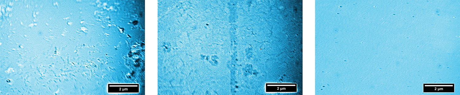
The entire process was repeated several times with different target substrates commonly used in key electronic applications. Each time, the Raman spectroscopy revealed the same thing: purity, a high level of crystallinity, and single-atom thickness. The same analysis for thermal release tape and PMMA, however, continued to turn up evidence of unwanted residue. Not significantly limited by time, cost, or size, the new method should make possible a whole fleet of emerging technologies.
“One of the best things about it,” Dervishi says, “is that there are no size limitations. The graphene sheets can be made any size, for virtually any application, and the process should work just as well.”
Potential Applications
- Computer processors and memory chips
- Waterproof coatings
- Inexpensive thin-film solar panels
- Electrically conducting ink
- Selective transport membranes (e.g., for carbon sequestration or water desalination)
- Infrared-vision contact lenses
- Medical diagnostic instruments, tissue engineering, and drug delivery
- Advanced pressure sensors
- Flat or flexible touch screens for phones, tablets, and other devices
- Research for spintronic and quantum computers
- Long-lived, quick charging, and lightweight batteries and supercapacitors