Designing quantum dots for light, energy, and emerging quantum technologies
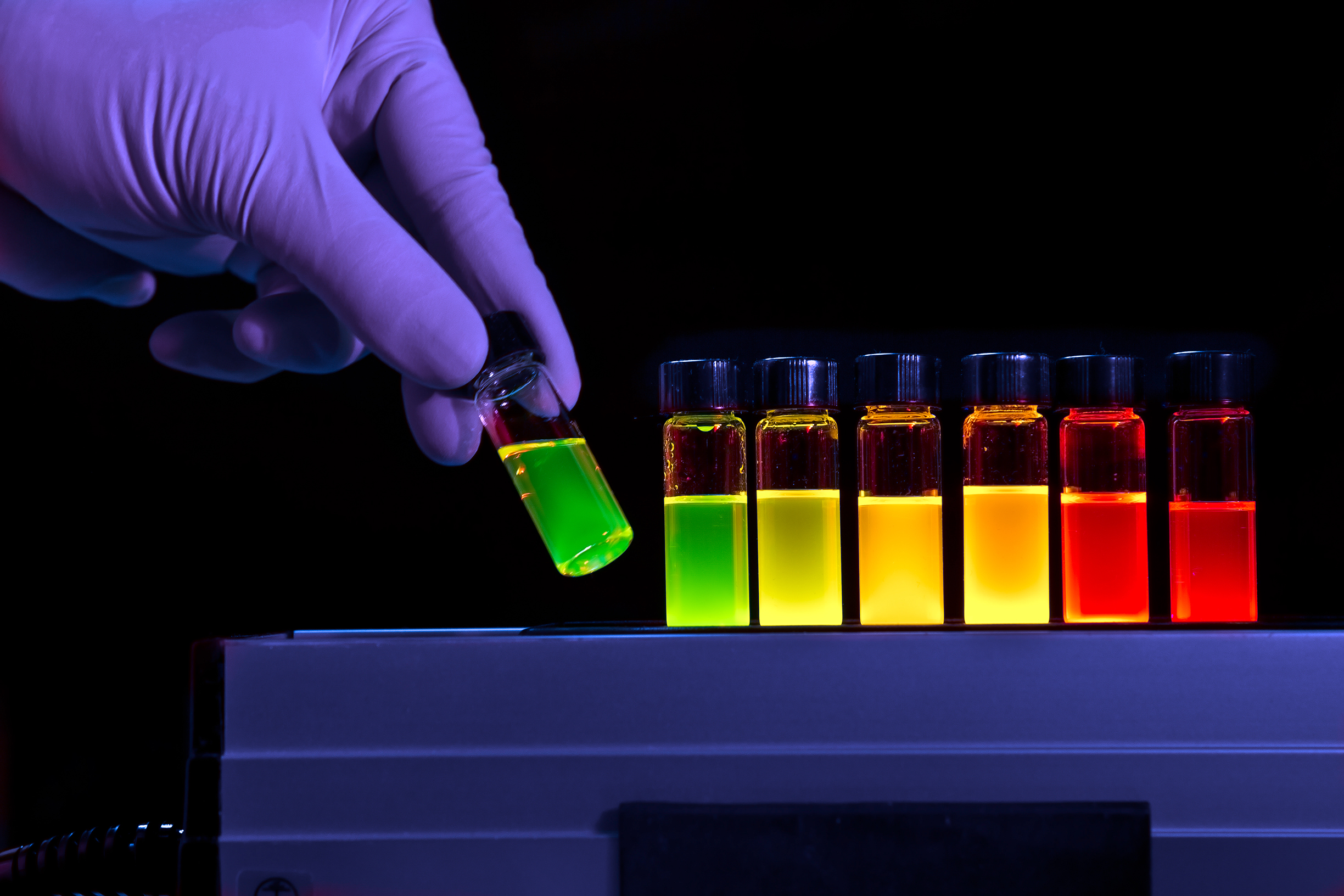
Our team focuses on the synthesis, electronic and optical properties, and device applications of semiconductor nanocrystals—also known as colloidal quantum dots (QDs). By precisely controlling composition, size, shape, and surface chemistry, we engineer quantum dots with tailored electronic structure and designed functionality. Our research spans advanced nanomaterial synthesis, state-of-the-art ultrafast and single-particle spectroscopy, and integration into electronic, optoelectronic and photonic devices. Leveraging the exceptional versatility of colloidal nanocrystals, we explore new frontiers in nanotechnology, photophysics, and energy conversion.
Experimental Capabilities
Synthesis, Materials Characterization, Advanced Optical Spectroscopy, and Device Fabrication
Our research leverages the extensive, state-of-the-art experimental capabilities spanning materials synthesis, characterization, spectroscopy, and device fabrication. Together, these resources provide an integrated platform for the development and investigation of quantum-dot-based materials and devices.
Synthesis
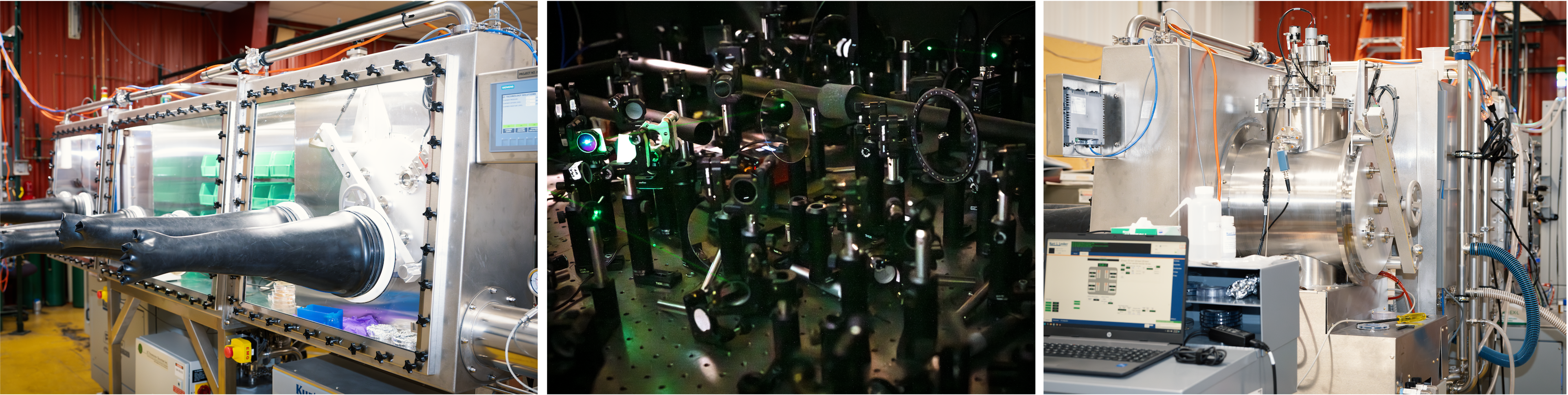
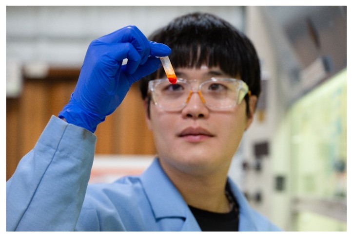
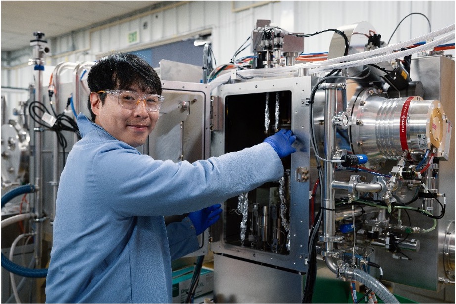
The team operates a fully equipped chemistry laboratory dedicated to the synthesis of colloidal nanomaterials. The facility includes five chemical fume hoods and two inert-atmosphere glove boxes, enabling the preparation of air- and moisture-sensitive materials. The laboratory is optimized for the controlled colloidal growth of semiconductor quantum dots, including core-only, core/shell, heterostructured, and doped nanocrystals.
To support rapid synthetic optimization, the laboratory also houses several in-house characterization tools that provide immediate feedback on materials properties. These include a UV–Vis absorption spectrometer, a fluorimeter with time-resolved capability, a system for elemental analysis by inductively coupled plasma (ICP) spectroscopy, and a scanning electron microscope (SEM).
Materials Characterization
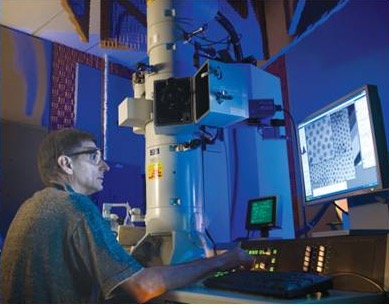
Materials characterization capabilities encompass a comprehensive suite of tools for elemental, structural, and microstructural analysis, as well as detailed assessment of optical and spectroscopic properties. These include a high-precision inductively coupled plasma (ICP) emission spectrometer for elemental composition analysis; scanning electron microscopy (SEM) and high-resolution transmission electron microscopy (TEM) for nanostructure imaging; and atomic force microscopy (AFM) and scanning tunneling microscopy (STM) for surface morphology and thin-film characterization.
In addition to standard instruments for optical absorption and emission measurements, the team maintains multiple advanced systems for time-resolved and single-quantum-dot spectroscopy (see dedicated spectroscopy webpage). Together, these capabilities provide comprehensive insight into the composition, structure, optical properties, and functional performance of synthesized nanomaterials.
Spectroscopy
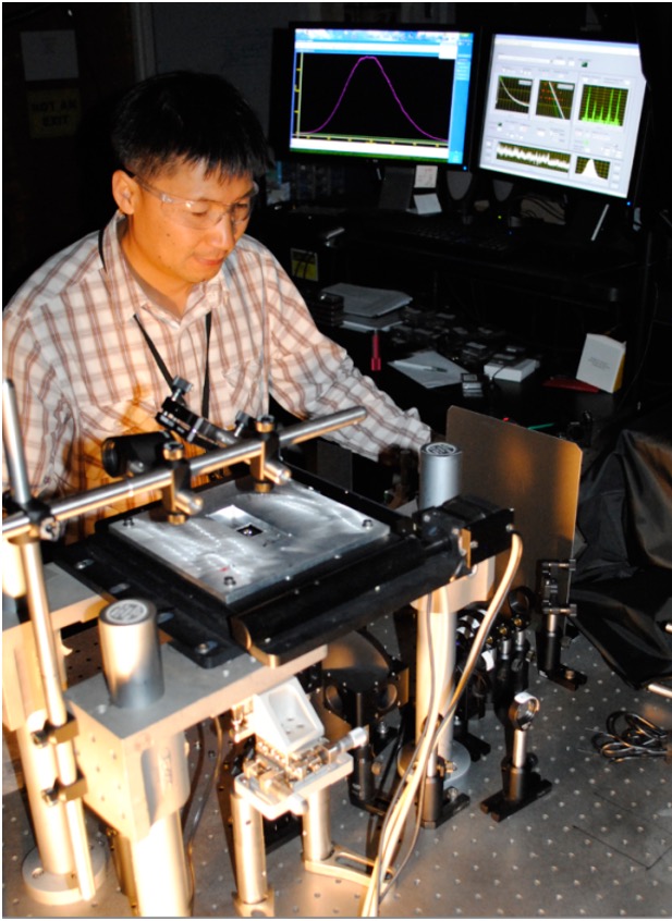
The team maintains three optical laboratories dedicated to advanced ultrafast, single-particle, and magneto-optical spectroscopy. These facilities house six amplified femtosecond laser systems and multiple optical parametric amplifiers (OPAs), enabling experiments spanning the near-infrared to ultraviolet spectral range. Detection capabilities include four superconducting nanowire single-photon detectors with ~40 ps temporal resolution, as well as two custom-built single–quantum-dot micro-photoluminescence (µ-PL) systems.
Additional instrumentation includes two broadband femtosecond transient absorption spectrometers, a femtosecond photoluminescence upconversion system, a picosecond streak camera, and a setup for transient photocurrent spectroscopy. The laboratories also feature an optical cryostat equipped with a 7-T superconducting magnet, supporting magneto-optical studies, including ultrafast magneto-optical spectroscopy. Collectively, these tools enable detailed investigations of ultrafast carrier, exciton, spin, and charge dynamics, which are critical for understanding nanostructure functionality and guiding the optimization of material properties.
Device Fabrication
Device fabrication capabilities include a two-chamber thin-film deposition system capable of processing both organic and inorganic materials, an electron-beam lithography (EBL) system, thermal evaporation and magnetron sputtering systems, and multiple spin coaters. Additional tools include an atomic layer deposition (ALD) system, an oxygen plasma etcher, and equipment for screen printing and electrophoretic deposition. Together, these capabilities support the fabrication of exploratory quantum-dot-based photoconductive, optoelectronic, and photonic devices.
Research Areas
Over three decades of quantum dot research at Los Alamos, driving advances in quantum dot synthesis, spectroscopy, and optoelectronic devices.
Engineered Nanomaterials
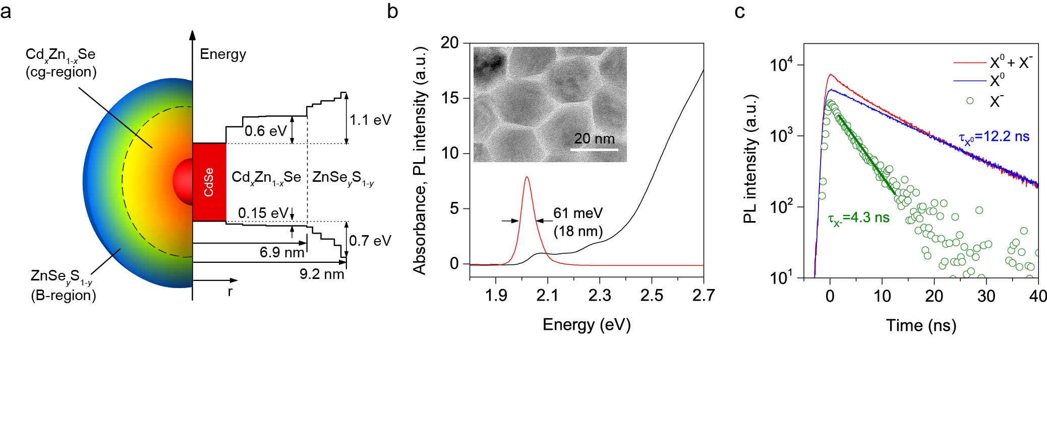
Continuously graded QDs with strongly suppressed Auger recombination and sub-thermal linewidth for LEDs, lasers and single-QD light sources. www.nature.com/articles/nmat5011
Our materials development efforts aim to enable next-generation quantum dot functionalities by achieving precise and programmable control over their electronic, optical, and magneto-optical properties. We pursue this goal through:
Rational control of size, shape, and composition to engineer quantum confinement and band structure
Compositional grading and heterostructure design to tailor carrier dynamics and interfacial processes
Advanced surface chemistry and passivation strategies to control charge transport and environmental coupling
Magnetic, electronic, and optical doping to introduce new spin, charge, and light-matter interactions
Intentional incorporation and control of functional defects as active elements for emerging device concepts
Exploratory Devices
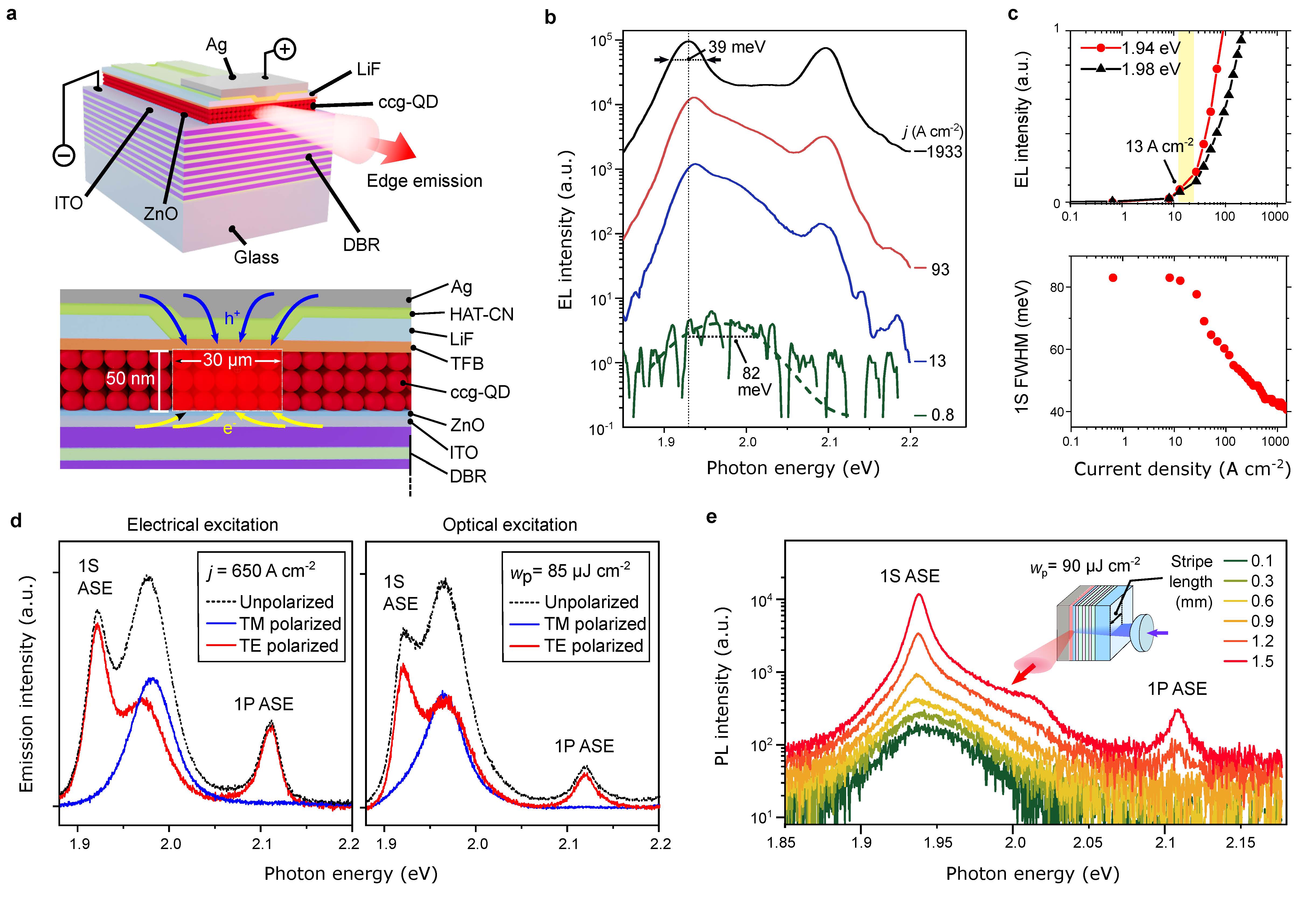
Electrically driven amplified spontaneous emission (ASE) in a high–current-density LED with an integrated Bragg-reflection waveguide—an important milestone toward a colloidal QD laser diode. www.nature.com/articles/s41586-023-05855-6
Our device-oriented research exploits the unique properties, versatility, and tunability of colloidal quantum dots to realize new classes of solution-processed devices. These efforts target applications spanning light emission, energy conversion, electronics, optoelectronics, photochemistry, and emerging quantum technologies. Current focus areas include:
Quantum dot lasers, laser diodes, and LEDs
Photocathodes and electron emitters for photochemical applications
Single–quantum-dot light sources for quantum optics
Luminescent solar concentrators and photovoltaic devices
Photodetectors, including ultrafast Auston-switch platforms
Novel Physical Phenomena and Advanced Spectroscopy
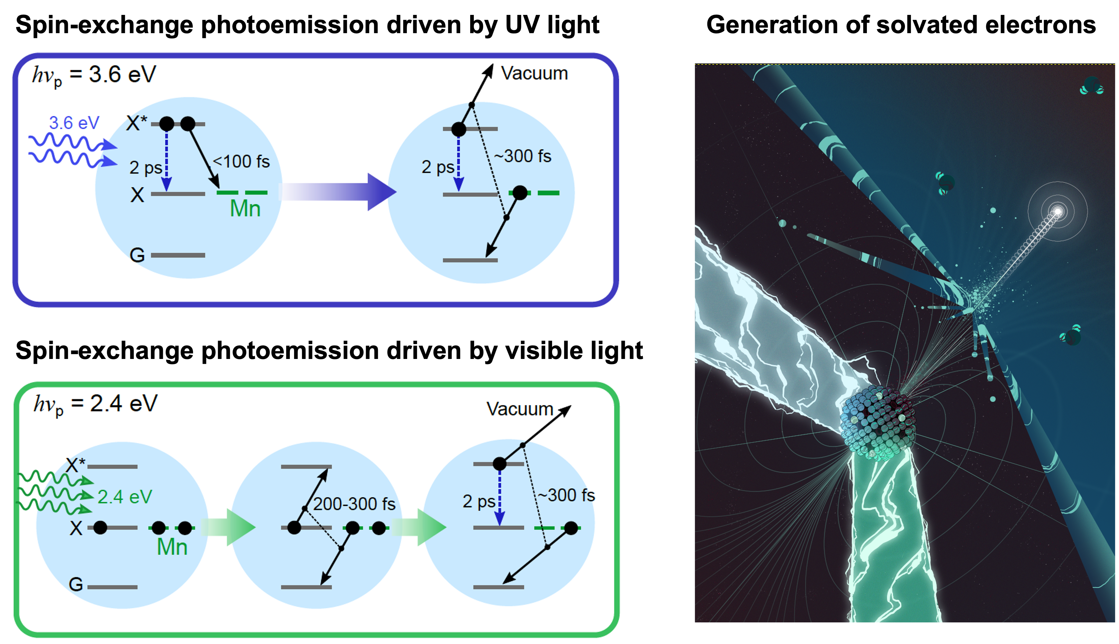
Highly efficient electron emission enabled by ultrafast (~100 fs) spin-exchange Auger up-conversion in manganese-doped quantum dots, with applications in photocathodes, photochemistry, and advanced photoconversion. www.nature.com/articles/s41566-022-00989-x
Our research explores unique physical phenomena that emerge in the nanoscale confinement regime, leveraging state-of-the-art ultrafast, magneto-optical, and single–quantum-dot spectroscopies. Current efforts focus on understanding and controlling:
Multi-carrier interactions and ultrafast dynamics, including Auger processes
Light emission and optical gain under both optical and electrical excitation
Interfacial charge and exciton transfer across hybrid nanostructures and QD-molecular assemblies
Ultrafast spin-exchange phenomena and spin-dependent dynamics