Electroplated Materials and Array Design for Scintillators
A scalable method for fabricating high-resolution, high-Z scintillator grids using electroplating and hot isostatic pressing
technology Snapshot
Overview
Modern scintillator grids are essential to radiation detection systems that require high spatial resolution and fast response. However, current grid fabrication methods rely on hazardous chemical etching and produce inconsistent structures that limit performance, scalability, and safety. This capability addresses the limitations of current fabrication methods by eliminating hazardous chemical etching, improving uniformity, and enabling complex geometries at scale.
Advantages
- Enables high-resolution grid fabrication from high-Z metals (e.g., Re, Au, Re/Ni)
- Avoids toxic and hazardous chemicals associated
with traditional etching - Supports scalable production of precision-aligned, high-Z scintillator arrays with low material loss
- Provides micron-level dimensional control and
uniformity - Compatible with multiple scintillator materials and array configurations, enabling customization for
medical, industrial, and defense applications - Adaptable to custom geometries for specialized imaging or detection applications
Technology Description
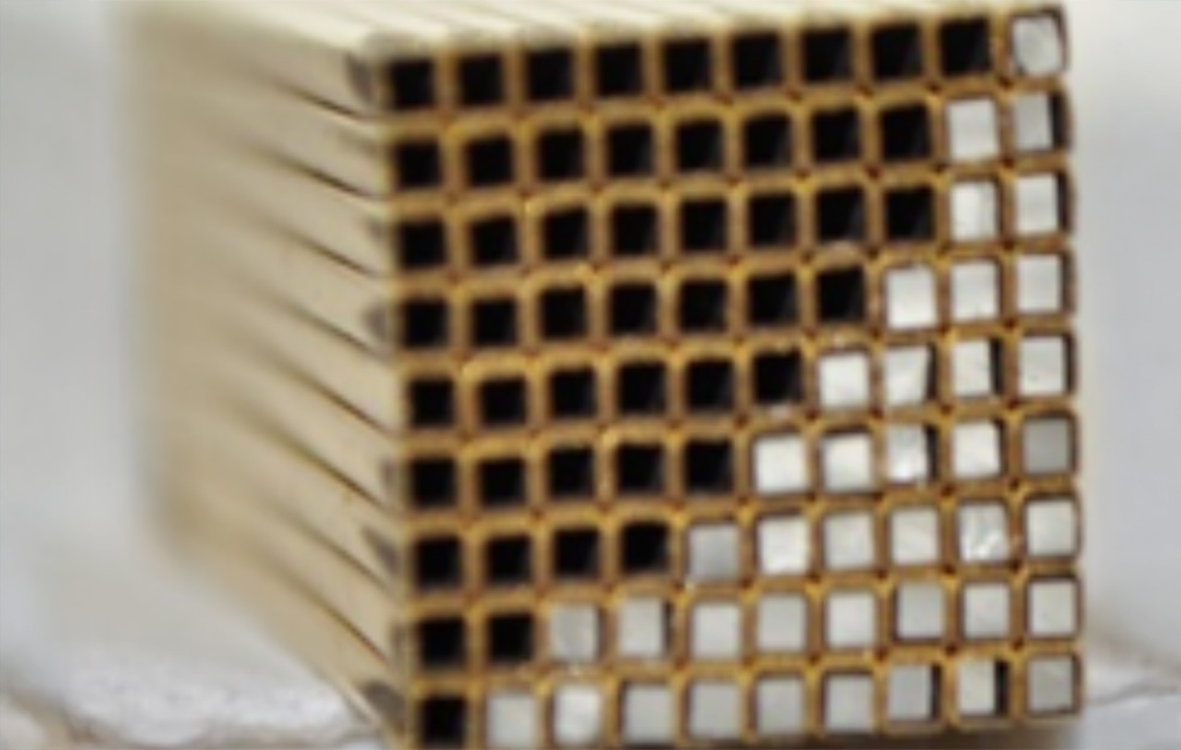
This technology enables the fabrication of dense, high-resolution scintillator grid arrays with micron-level precision, suitable for advanced radiation detection and imaging applications. The process works by electroplating high-Z metals, such as rhenium (Re), gold (Au), or their alloys, onto a substrate in the shape of the final grid geometry. These electro-formed components are then joined using hot isostatic pressing (HIP) at metal-specific temperatures and pressures to form solid bonded structures. Finally, the substrate is dissolved, leaving behind a free-standing, precision-aligned grid array. This approach eliminates chemical hazards, improves feature uniformity, and supports complex geometries, making it suitable for both small- and large-scale detector production.
Market Applications
This technology supports next-generation imaging and detection systems where high resolution, precision fabrication, and material efficiency are critical. This process can benefit:
- Fabricating CT, PET, and SPECT detector arrays for medical imaging
- Developing radiation detection systems for homeland security or military use
- Producing NDT imaging systems for aerospace and industrial inspection
- Supporting nuclear energy monitoring with compact, rugged detection grids
- Enabling advanced materials R&D for photonic and meta-material applications
Next Steps
Advancing toward production readiness through validation across multiple metals and configurations. Development is focused on scaling production, refining substrate removal protocols, and aligning grid architectures with commercial detector specifications. Partner-led efforts will help demonstrate performance in application-specific systems and adapt the method for custom geometries and material combinations.


