Optics and Engineering
Contact
- Aaron Anderson
Our team has developed sensors from the conceptualization to the development of a prototype research instrument. This process includes the development of electronics, optics, mechanical design and fabrication.
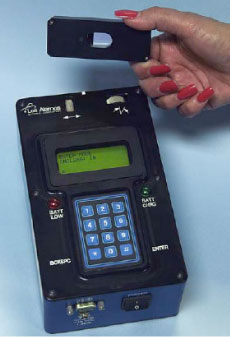
One example of such an effort is the bench top research instrument, which employs planar optical waveguides as the sensing platform. This bench top instrument was then engineered into a handheld unit, a progression toward the next steps of commercialization and broader use. We are working on instruments that use optical (fluorescence), interferometric, and impedance read-outs.
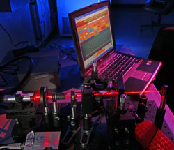
- Left: Bench-top waveguide instrument
- Right: Engineered handheld waveguide instrument
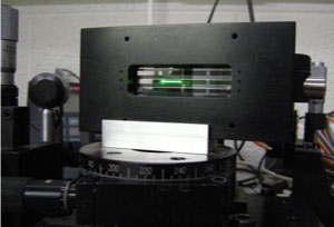
The multichannel waveguide consist of a 76.2mm diameter 2mm thick fused silica optically polished substrate (low index n=1.46) and a Si3N4 high index film (n=1.81) 110nm +/- 5nm thick. The very thin waveguide film requires the use of detractive grating elements for coupling light into the waveguide. The grating coupler elements are fabricated using a holographic interference technique to generate the periodic pattern (for a wavelength of 532nm and a +10 degree coupling angle the period is 420nm). That pattern is etched into the substrate surface by a reactive ion etching (REI) process. The gratings are actually fabricated prior to the deposition of the waveguide film. The grating is etched into the substrate and subsequently over coated with the Si3N4. To ensure the gratings are not effected by ambient refractive index changes, the grating coupler region must also be over coated with a layer of dense SiO2 that is 1100nm or thicker, thus isolating the evanescent field from the surrounding media. In addition to the Si3N4 waveguiding film, a thin SiO2 film, thickness of 10nm, is deposited on the waveguide surface sensing area, which provides the functional groups required for covalent attachment of an appropriate sensing chemistry.
The multichannel waveguide consist of three channels with four sensing elements per channel. Each sensing element is 10mm long and 1.5mm wide and has a 1.5mm x 1.5mm detractive grating element which enables each sensing element the ability to be excited independently of each other. The channels and sensing elements also have a chrome absorbing material surrounding them, allowing each element to be excited independently with out cross talk or inadvertent coupling between the sensing elements. After the waveguide coatings have been deposited on to the substrate, the substrate is cut to 76.2mm x 25.4 mm. Cutting the substrate to these dimensions permits the substrate to be incorporated into a flow cell and mounted into a holder for the addition of reagents. The flow cell consist of the multichannel waveguide substrate, a laser cut three channel 0.5mm thick silicone rubber gasket and a glass cover with dimensions of 76.2mm x 25.4mm x 1mm with six holes bored into it at precise locations to align with the individual channels. The flow cell is captured in a holder which incorporates septum material to form a seal with the glass cover and allow the addition of reagents via a syringe and be integrated into our experimental apparatus for measurement and detection. This configuration minimizes reagent volumes (100μl/channel), is self sealing, and allows the addition of multiple reagents. The multichannel waveguides provide the ability to do three separate assays in quadruplet for each channel.
